Random Numbers on a Homebrew FPGA CPU
Using a Galois LFSR PRNG on a custom 8-bit CPU in an FPGA, wired up with IN and OUT instructions

The CPU Project
As I wrote about previously, I have been building an 8-bit CPU in Verilog, synthesized onto an Intel MAX1000 FPGA. The project cpu_in_fpga is a simple CPU with 8 general-purpose registers, a hardware stack, an ALU.
I wanted the programs you can run on it: "to do something" (the functional programmer in me would say: It needs to have side effects)
Typically this is done through dedicated IN and OUT instructions. where the assembly program can access peripherals via port assignments (each port resembles a certain peripheral, like GPIO ports, an Analog Digital Converter, the 8 LED's on the board, etc)
One of those peripherals I built is a pseudo-random number generator (PRNG), as any cpu will benefit from some randomness.
This post walks through how it works, how the assembly program talks to it, and what you can see when it runs.
The Galois LFSR
The PRNG is implemented as an 8-bit Galois Linear Feedback Shift Register (LFSR). An LFSR is a shift register where some of the bits are fed back through XOR gates to produce the next state. The "Galois" configuration places those XOR gates inside the register, in parallel making it fast in hardware.
The specific polynomial used here is:
x⁸ + x⁶ + x⁵ + x⁴ + 1 → tap mask 0xB8
In Verilog the next-state logic is just three lines:
wire feedback = lfsr[0];           // output bit (LSB)
wire [7:0] shifted = lfsr >> 1;    // shift right
wire [7:0] next = feedback ? (shifted ^ TAP_MASK) : shifted;
Each clock cycle the register shifts one position to the right. When the outgoing LSB is 1, the tap positions (bits 7, 5, 4, 3 are the set bits of 0xB8) are XORed with the shifted value. When it is 0, no XOR happens and the register just shifts.
This polynomial is maximal-length: starting from any non-zero seed it visits all 255 non-zero 8-bit values before cycling back. Zero is the only forbidden state as it would just keep shifting right, never ever changing, the PRNG circuit guards against it by silently replacing a seed of 0x00 with 0x01.
The LFSR runs on the 12 MHz board clock, independent of the CPU clock. The CPU runs at a divided-down rate, so every time the program reads the PRNG it samples a different phase of the sequence. The values are not cryptographically random, but they look completely unpredictable from the assembly program's point of view.
IN and OUT Instructions
The CPU has two instructions for communicating with peripherals:
| Instruction | Encoding | Operation |
|---|---|---|
IN Rd, port | 1000 ddd ppp xxxxxxxx | Rd = peripheral[port] |
OUT Ra, port | 1001 aaa ppp xxxxxxxx | peripheral[port] = Ra |
The relevant port assignments are:
| Port | Peripheral | IN | OUT |
|---|---|---|---|
0x01 | PRNG | Read current LFSR value | Seed / reseed the LFSR |
0x02 | Onboard LEDs | Set all 8 LEDs at once |
Reading the PRNG (IN Rd, 0x01) samples the 8-bit LFSR value at that instant.
Seeding the PRNG (OUT Ra, 0x01) loads the value in Ra directly into the LFSR. At power-on the hardware already seeds it from a free-running counter so that each reset starts at a different point, but the program can override that at any time.
Driving the LEDs (OUT Ra, 0x02) writes all 8 bits of Ra directly to the eight on-board LEDs. The LED register holds its state until the next write.
The program
; prng.asm  hardware PRNG demo
; clk_div: 20
; name: Random
;
; Reads the FPGA programmed Galois PRNG and displays each value on the LEDs

.equ PRNG_PORT,    0x01
.equ LEDS_PORT,    0x02
.equ INITIAL_SEED, 0x2A

        LDI  R0, INITIAL_SEED     ; load seed value (42 decimal)
        OUT  R0, PRNG_PORT        ; write seed into the LFSR

loop:
        IN   R7, PRNG_PORT        ; sample current LFSR value
        OUT  R7, LEDS_PORT        ; show it on the LEDs
        JMP  loop                 ; repeat forever
Let's step through it:
LDI R0, INITIAL_SEED Load Immediate. Puts the value 0x2A (decimal 42) into register R0. This is the starting seed.
OUT R0, PRNG_PORT Write R0 to port 1. This reseeds the LFSR with 0x2A, giving the sequence a deterministic starting point (on top of the hardware seed already applied at reset).
IN R7, PRNG_PORT Read port 1 into R7. Because the LFSR is running at 12 MHz and the CPU clock is divided down by 20 (the clk_div: 20 header directive), a meaningful number of LFSR cycles have elapsed since the last read. The value in R7 is effectively a fresh random byte every iteration.
OUT R7, LEDS_PORT Write R7 to port 2. The 8 LEDs instantly reflect the new random value.
JMP loop Unconditional jump back to loop. The program runs forever.
The result is a visually chaotic light pattern: each LED appears to toggle independently, with no visible periodicity.
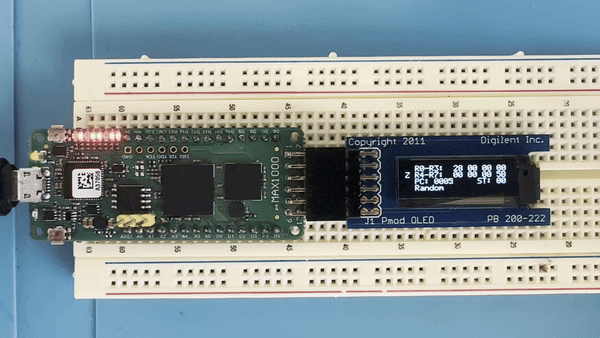
In Action
Here you see on the display register R7 being filled with the random number and the LEDS on the left display the binary version of it.
Conclusions
A few things stand out from this tiny program:
Hardware peripherals keep assembly programs simple. The LFSR logic feedback polynomial, maximal-length sequence, zero-lock guard is entirely in the RTL. The assembly programmer just reads a port. Eight lines of assembly are enough to drive a seemingly random light show.
Clock domain separation is a feature. By running the PRNG on the board clock instead of the CPU clock, the sampling phase is always different. A synchronous PRNG clocked at the same rate as the CPU would return the same value on every read if the CPU read it every cycle. The asynchronous design sidesteps that entirely.
The IN/OUT instruction pair is a clean peripheral interface. No memory-mapped registers, no special addressing modes one instruction to read, one to write. For a small embedded CPU this keeps the decoder and the assembly programmer's mental model both straightforward.
Seeding matters. The hardware seeds from a free-running counter at reset, but the program adds its own seed on top. For any application where reproducibility is useful (testing, procedural generation with a known seed) you can control the sequence completely. For applications where you want maximum apparent randomness, you can skip the OUT and rely on the hardware seed.
The full project, including the Verilog RTL, assembler, and all example programs, is at github.com/gertjana/cpu_in_fpga.